Weitere Unterabschnitte: Chip-Herstellung | Halbleitertechnologien | Wire-Bonding | Bestückung
Computerindustrie
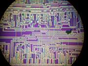
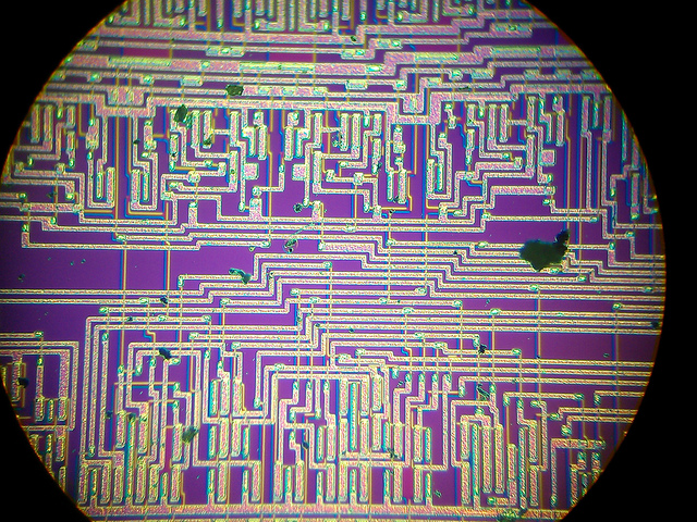
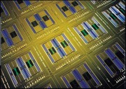
Wafer in Darkfield

Bild: Carl Zeiss Microscopy
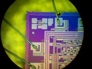
nebarnix – Flickr
-
- Microchip
-
- Microchip (2)
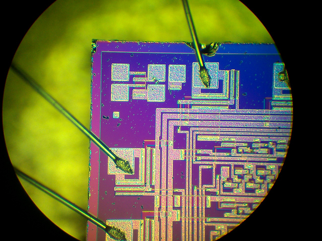
Bild: nebarnix
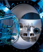
The ABB Group – Automation and Power Technologies
-
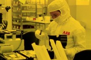
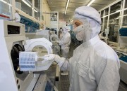
- Powerful semiconductors

-

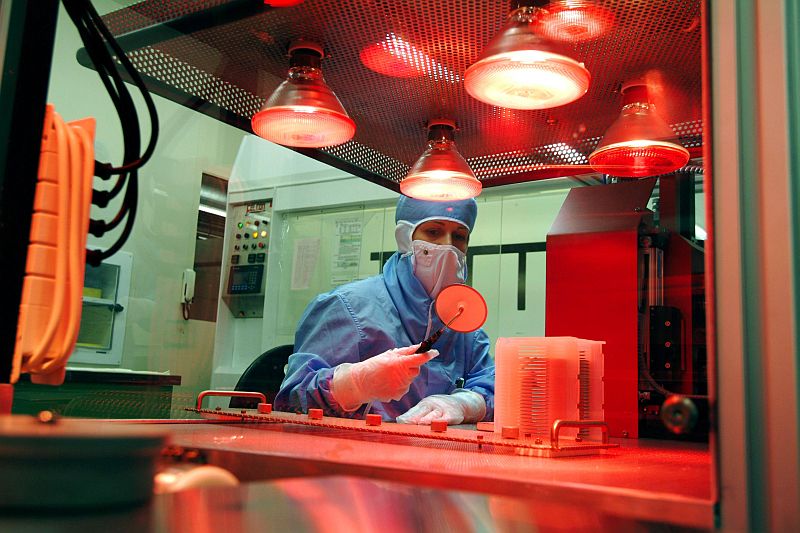
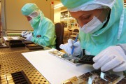
- Semiconductor production: Passivation
-
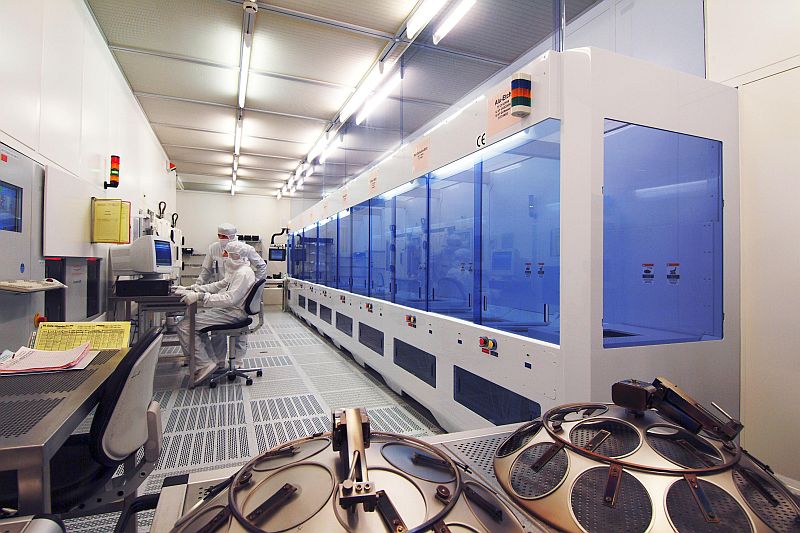
- Semiconductor production at ABB factory in Lenzburg, Switzerland (etching)
-
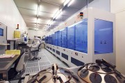
- Semiconductor production

-
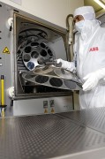
- Semiconductor production: Positioning

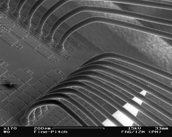
Wirebonding
x-ray of computer chip

Bild: tpmartins
Chip-Produktion / Planartechnik
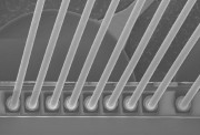
Wirebonding
Gold wire bonding
Chip-Produktion / Planartechnik
Bosch Pressebilder
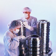
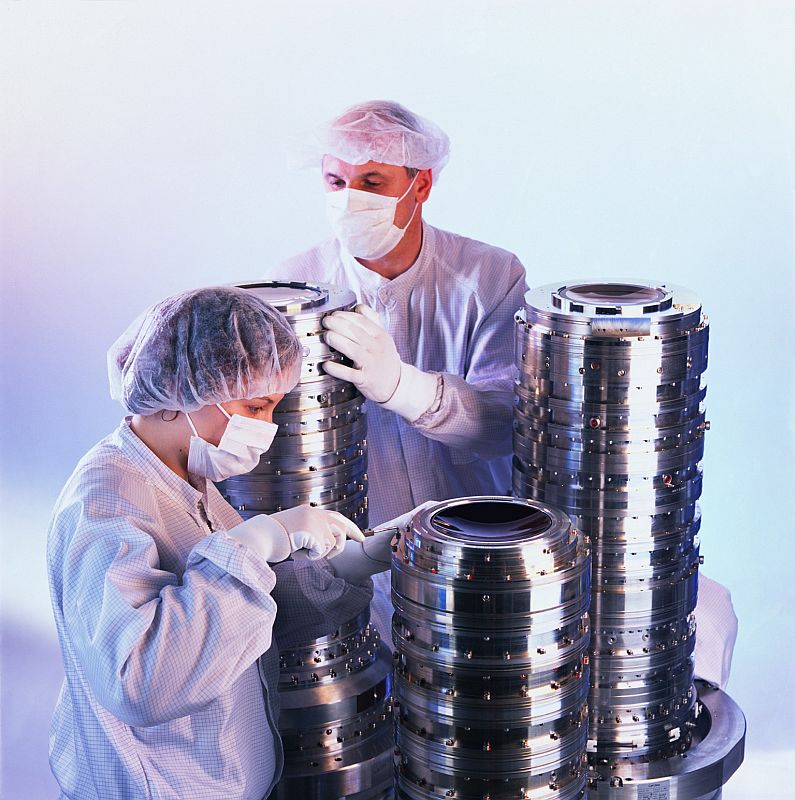
-
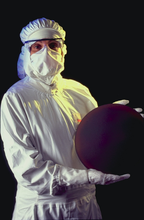
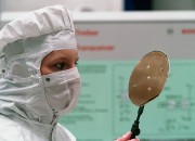
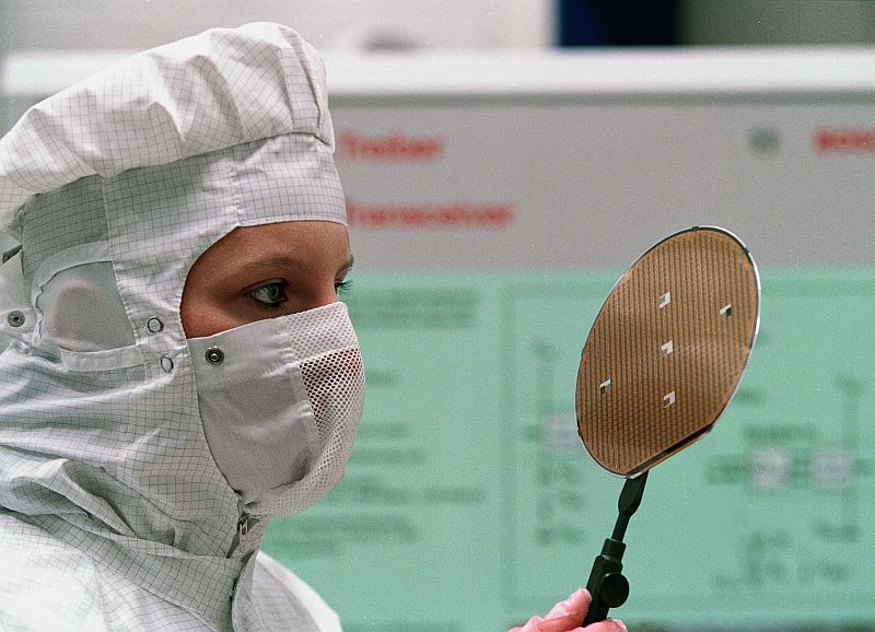
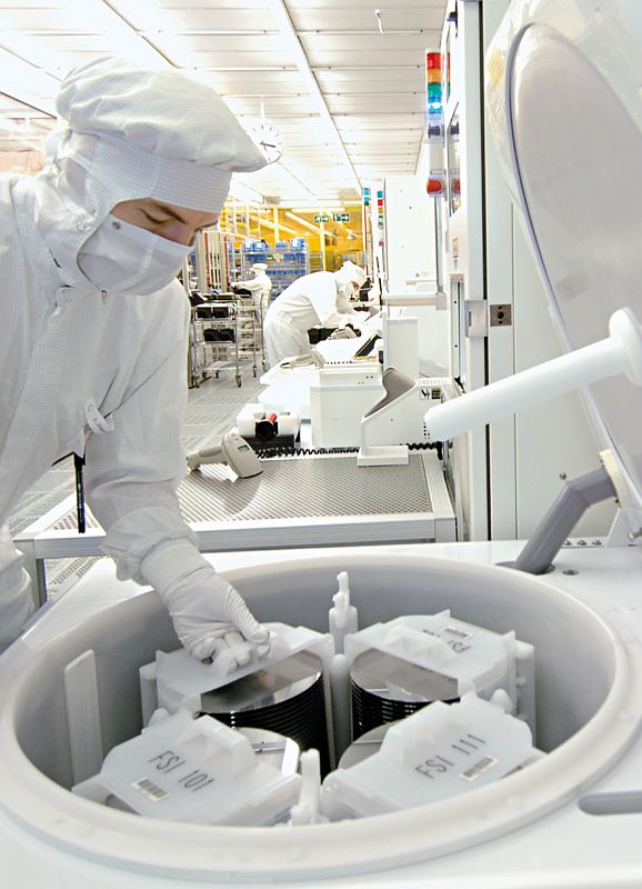
- Wafer mit einem Durchmesser von 200 Millimetern

-
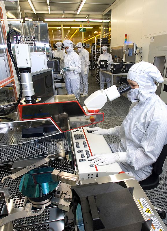
- Sichtprüfung eines 6-Zoll Wafers
-
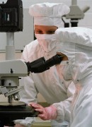
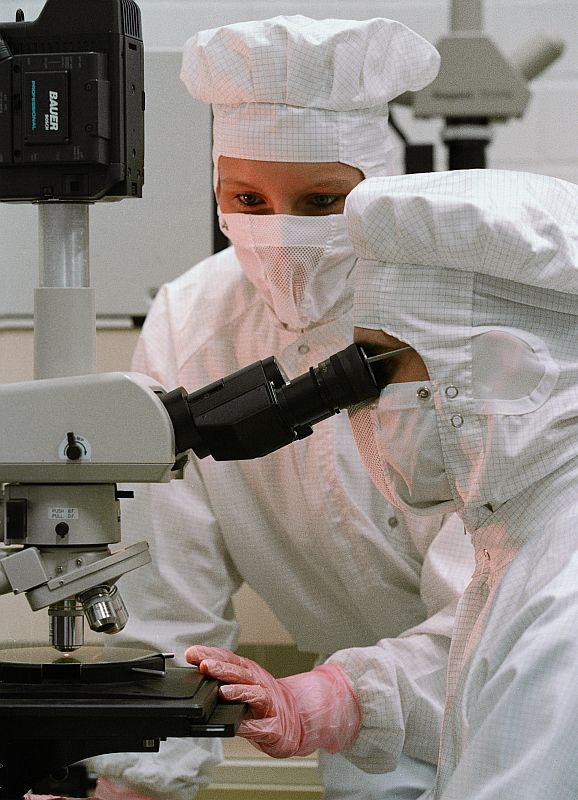
- Prüfung eines Wafers unter dem Mikroskop
-
- Mikromechanische Sensoren auf einem Silizium-Wafer

-

- Wafer
-
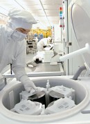
- Wafer mit einem Durchmesser von 200 Millimetern
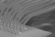
Wirebonding
Ultrasonic wire Bonding small clip
Wire Bonding
wirebond600.jpg
Chip-Produktion / Planartechnik
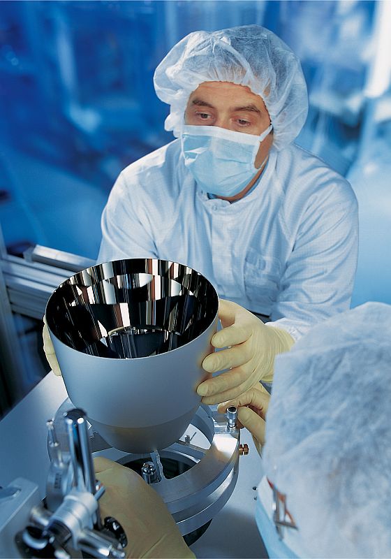
Carl Zeiss AG, Deutschland
-
- Raum für Präzisionsoptik

-
- Objektive für die Mikrolithographie
-

- Optik der Zukunft
Wirebonding
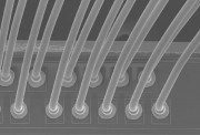
HITACHI Semiconductor
-

- 60um-1a.jpg
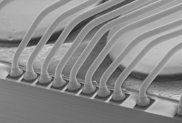
-
- 65um-1a.jpg
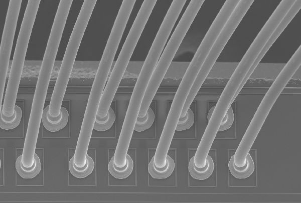
-
- 60um-3a.jpg

-
- 65um-2a.jpg