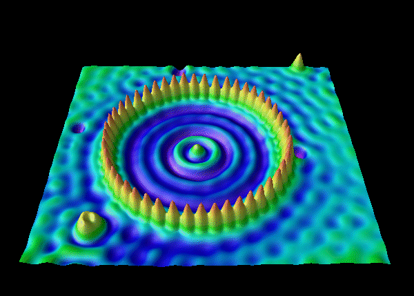
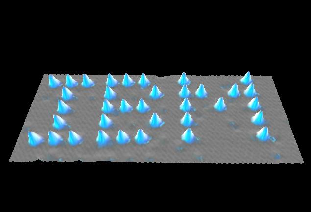
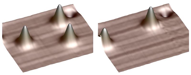
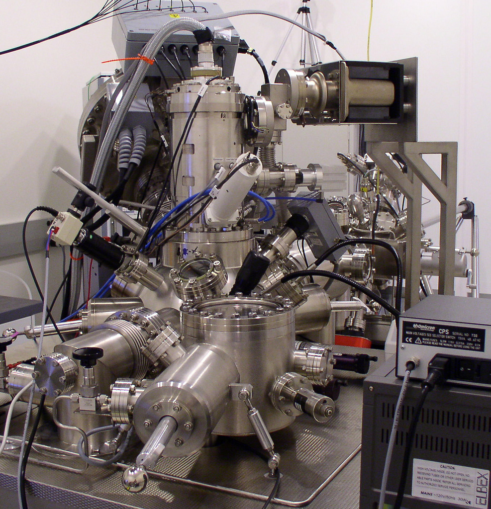
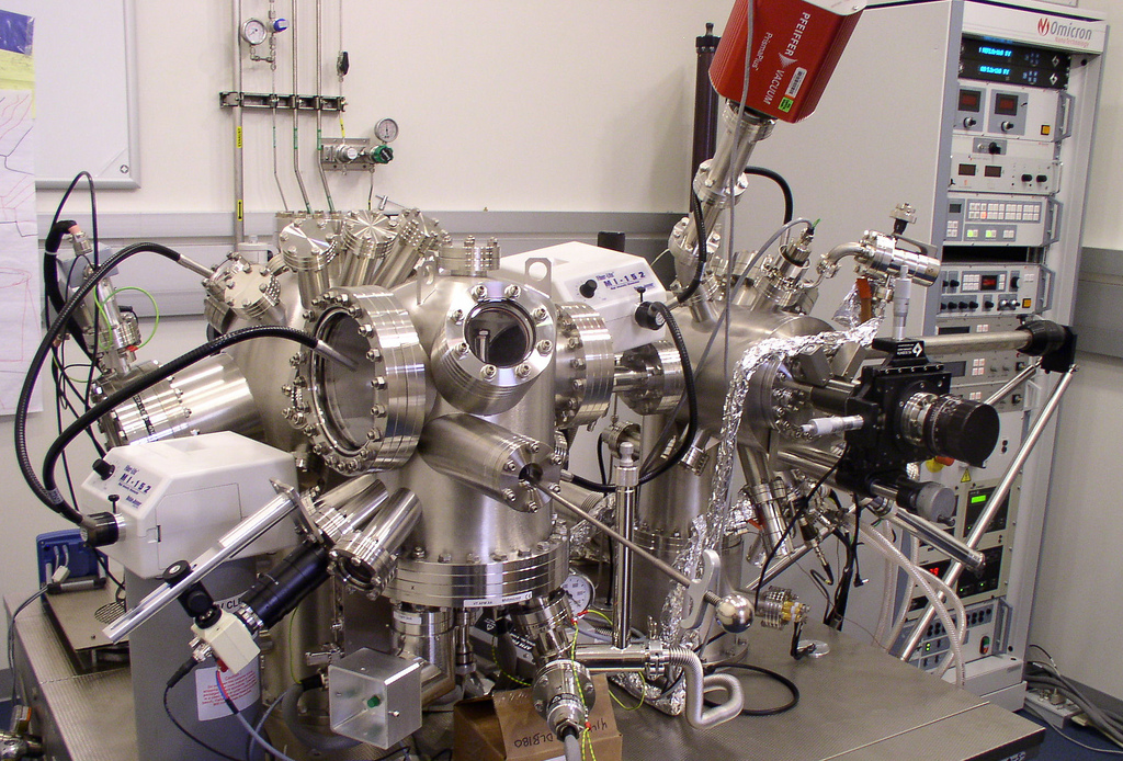
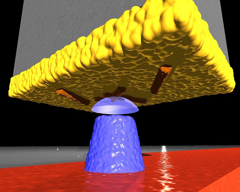
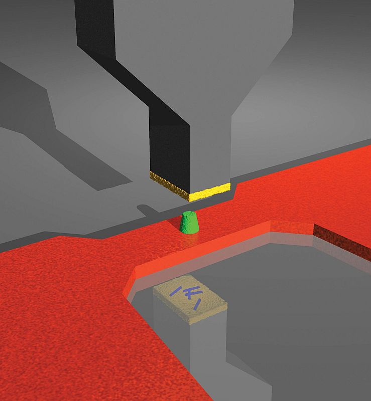
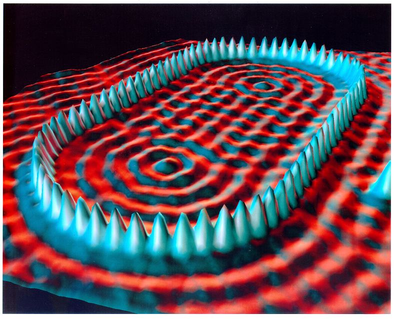
This atomic-sized image was created by IBM researchers and is part of an exhibit opening today at the United States Patent and Trademark Museum in Alexandria, Virginia. The image was made using scanning-tunneling microscope technology as part of an effort to pave the way for circuits made from atomic and molecular components.
Weitere Unterabschnitte: Biologie | Mikroskopie | Biotechnologie | Chemie | Physik | Physik 2 | Mikrokosmos | Nanokosmos | Wetter und Klima | Weltraum
Nanokosmos
Rasterkraftmikroskop
IBM Research: Scanning Tunneling Microscopy
Max Planck Gesellschaft – Ammoniakmoleküle werden mobil
Kupferoberfläche mit adsorbierten Ammoniak-Molekülen, aufgenommen mit einem Rastertunnelmikroskop.
Argonne National Laboratory – Flickr
IBM Press room – United States
weitere Anwendungen
Perfekt entspiegelt – Mediendienst 05-2010-Thema 3 – Fraunhofer-Gesellschaft
Perfekt entspiegelt (Bild)
Hydrogen sensor
Nanotechnologie: Innovationen für die Welt von morgen
Vom Sand zum Superchip: 300mm-Wafer für die Nanoelektronik
Magnetspeicher
Nanoscale vortices
Argonne materials scientist Mihaela Tanase observes a small magnetic disk with a transmission electron microscope. At Argonne's Center for Nanoscale Materials, Tanase discovered a new method to control the way the atoms in the magnetic disk orient themselves to form "nanoscale vortices,", which are illustrated on the computer screen.