The World’s Tiniest Art

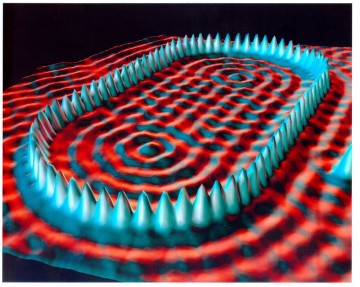
This atomic-sized image was created by IBM researchers and is part of an exhibit opening today at the United States Patent and Trademark Museum in Alexandria, Virginia. The image was made using scanning-tunneling microscope technology as part of an effort to pave the way for circuits made from atomic and molecular components.
