
Weitere Unterabschnitte: Chip-Herstellung | Halbleitertechnologien | Wire-Bonding | Bestückung
Computerindustrie
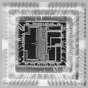
Chip-Produktion / Planartechnik
Wirebonding
Image13.gif
Chip-Produktion / Planartechnik
wafer.gif (Animation: 3 MB !)

Wirebonding
Intel inside
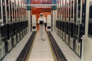
Photos — Intel Manufacturing Photos
-
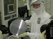
- Checking wafers processing

-
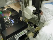
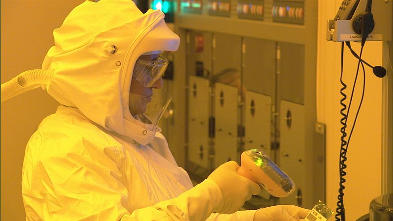
- A technician checks individual wafers

-
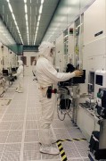
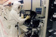
- Intel technicians monitor the wafers' progress
-
- application and removal of a light-sensitive polymer coating on silicon wafers

Silicon nanoelectronics and nanotech innovation
-
- Checking wafers processing
-
- A technician checks individual wafers
-
- Intel technicians monitor the wafers' progress
-
- application and removal of a light-sensitive polymer coating on silicon wafers
-
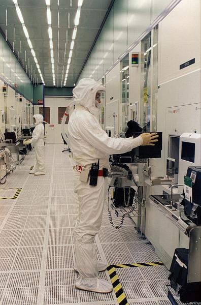
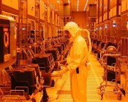
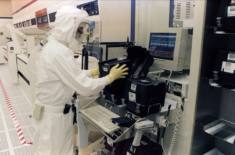
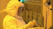
- Intel Fab workers in the cleanroom
-
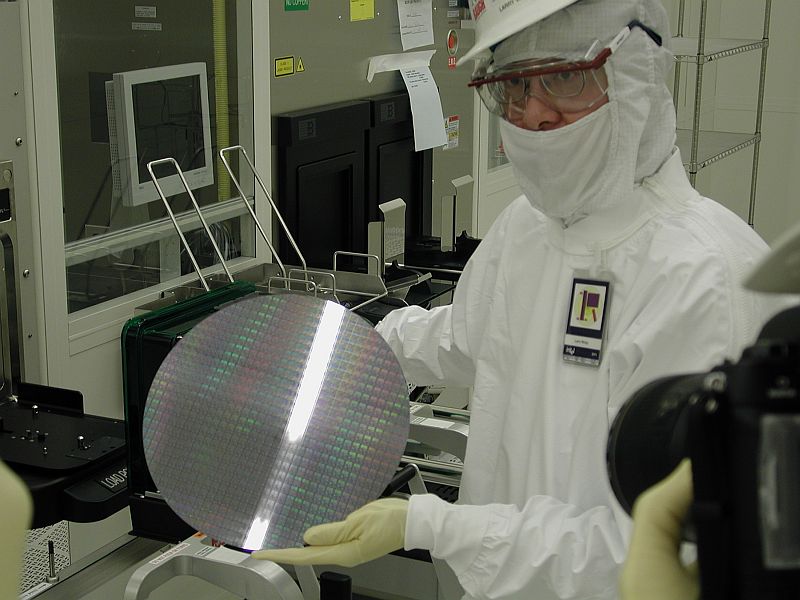
- An Intel technician holds a wafer for the camera.
-
- Intel technicians monitor wafers
-
- An Intel manufacturing technician
-
- Close up of the wafer as it spins during a testing procedure.
-
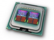
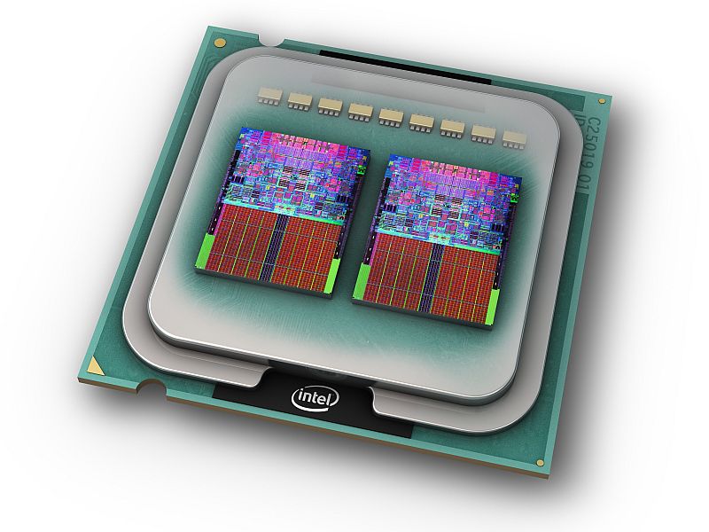
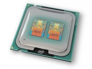
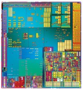
- Intel® Core™2 Extreme quad-core processor illustration
-
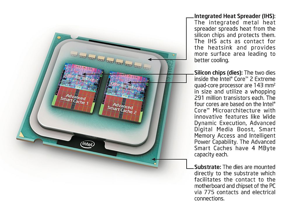
- Intel® Core™2 Extreme quad-core processor illustration with text
-
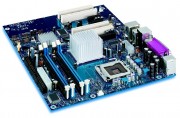
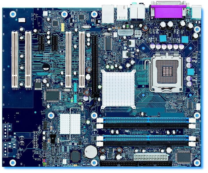
- Intel® D915PBL Motherboard
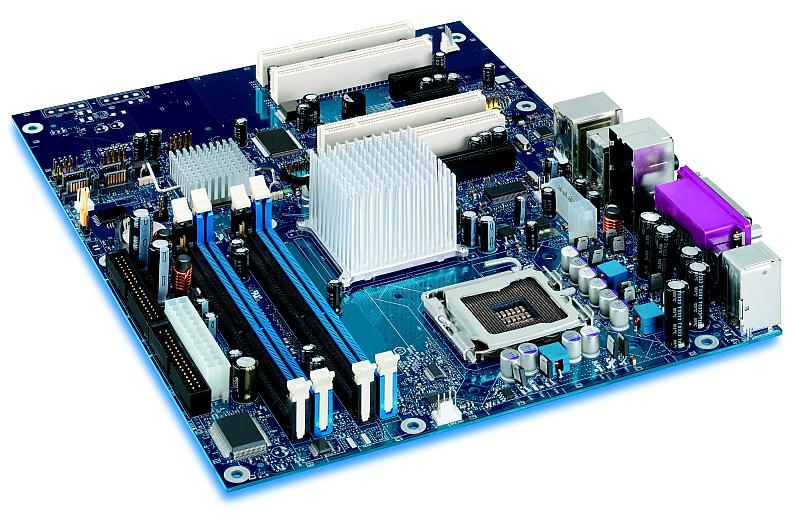
-

- Intel® D915PBL Motherboard
-
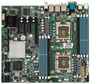
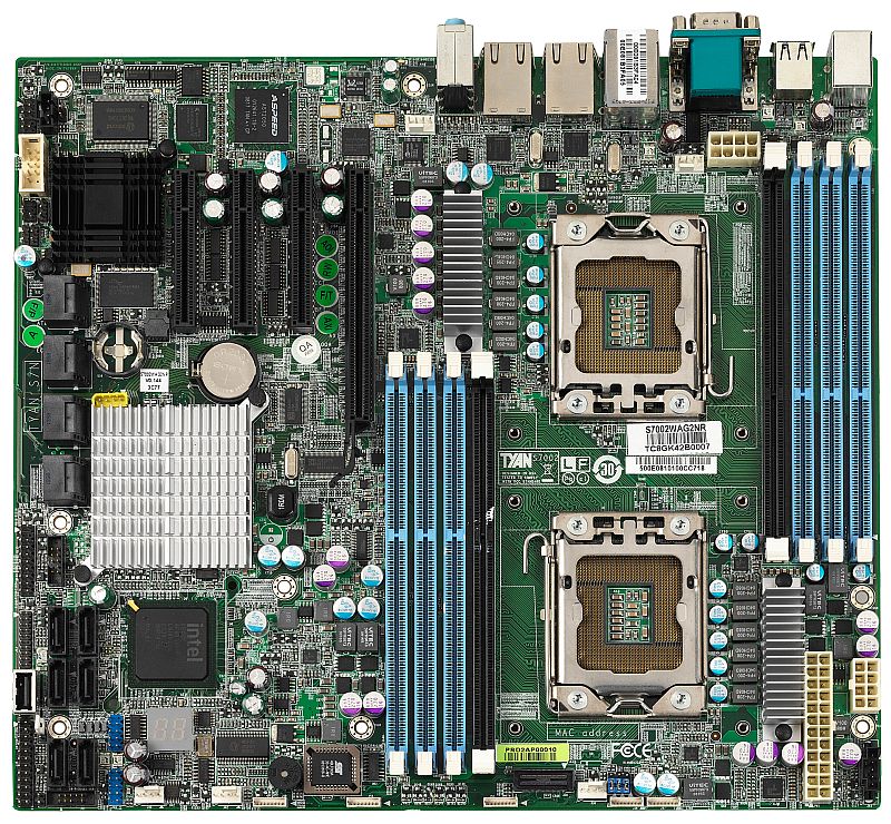
- Tyan S7002 motherboard
-

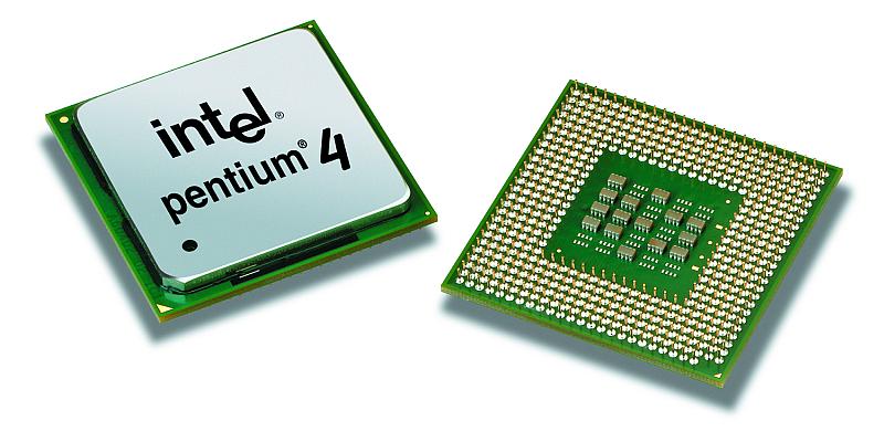
- Intel® Pentium® 4 Processor
-

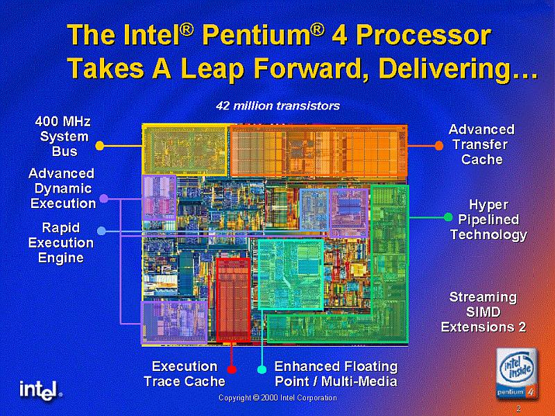
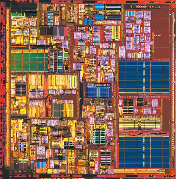
- Intel® Pentium® 4 Processor Die
-
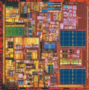
- Intel® Pentium® 4 Die on 0.13 Micron
-

- Intel® Pentium® 4 Die on 0.18 Micron
-
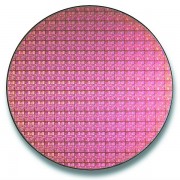
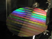
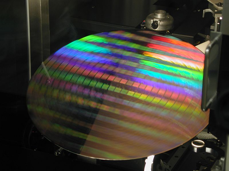
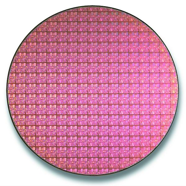
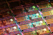
- Intel® Pentium® 4 Wafer on 0.13 Micron
-
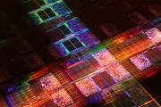
- Dunnington wafer shot

-
- Intel® Atom™ processor wafer

-

- Nehalem wafer shot
-
- Intel Peryn Quadcore Processor

-
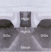
- Transistor with Hafnium-based high-k metal gate silicon technology
-
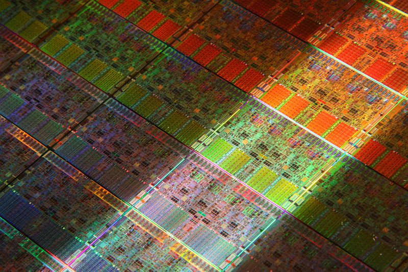
- Processors on an Intel 45nm "Penryn" Wafer

-
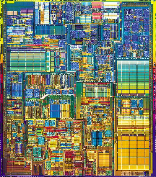
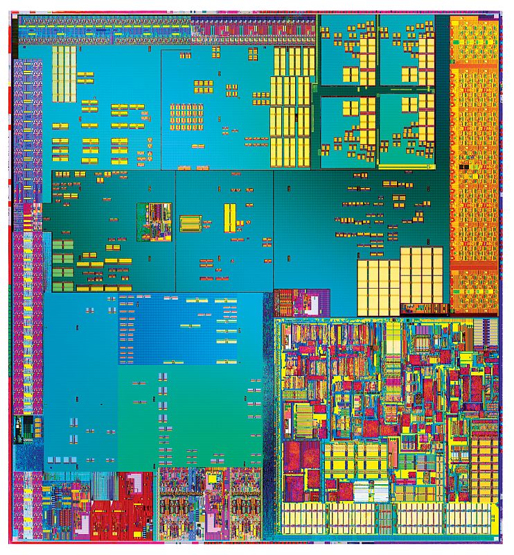
- Intel 45nm processor die

-

- Wafer containing Intel’s new Xeon 5500 series processors

-

- The Next Generation:Tulsa silicon wafer
-

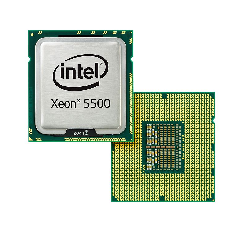
- Intel® Xeon® Processor 5500 Series
-
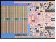
- Intel® System on Chip Die photo
-
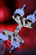
- First 40Gbps Silicon Laser Modulator
Strukturierung (Lithographie)
Interactive Java Tutorials: Building A Transistor
Herstellung von Transistoren mittels Planartechnik
Bild: LEIFI Physik